Designing Application-Specific Integrated Circuits
General-purpose processors are designed to handle a wide range of tasks, which makes them versatile but less efficient for specific applications. They face several challenges when compared to Application-Specific Integrated Circuits (ASICs),
What is an ASIC?
An Application-Specific Integrated Circuit is a type of circuit custom-designed to perform a specific function or set of functions. They provide high performance and efficiency for specialized applications. Despite the advantages, ASICs face several challenges, including high initial costs and long development cycles, making them primarily suitable for high-volume production.
Designing Application-Specific Integrated Circuits
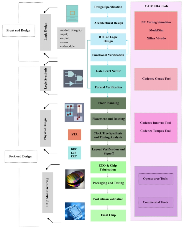
Design complexity is a primary challenge that involves increased verification efforts, power planning, and advanced packaging. Various steps in designing an ASIC are depicted in Fig. 1. This article provides a comprehensive overview of the ASIC design process, detailing the various steps from concept to production.
The ASIC design cycle is divided into frontend and backend domains, similar to software development. The front-end design deals with the visible aspects of the chip, such as its functionality and behavior. Backend design handles the hidden, physical aspects of the chip, such as layout and manufacturability.

Fig. 1 Design flow of application-specific integrated circuits Source: MDPI
Step 1: System Specification
It involves gathering information from stakeholders regarding the circuit's electrical and functional requirements. All the specifications, including I/O pins, functionality, power, dimensions, and how the chip should function under various scenarios, including environmental conditions, power consumption, and performance requirements, are all examined.
Step 2: Architectural Design
An outline of the chip's overall structure comprising a high-level block diagram and interconnect for every module is created.
Step 3: RTL Design
It is the step in the ASIC design flow where high-level behavioral descriptions of a system, often written in C, C++, or MATLAB, are automatically converted into register transfer level (RTL) code in Verilog or VHDL. RTL bridges the gap between high-level functional specifications and the physical implementation.
Step 4: Functional Verification
After the design has been implemented in HDL, simulations must be performed to verify that the circuit satisfies the required electrical specifications. It employs test benches like universal verification methodology (UVM), which are automated test protocols used to verify functionality and to identify and fix bugs before synthesis.
Step 5: Synthesis
During the logic synthesis phase, the RTL code is converted into a gate-level netlist that can be used for physical implementation. Converting RTL code into physical components collectively known as standard cells that are pre-designed building blocks such as logic gates, flip-flops, multiplexers, and buffers. Multiple optimizations are applied to enhance the final circuit's speed, area, and power efficiency.
Step 6: Formal Verification
Formal verification detects that a design adheres to its specifications and operates correctly under all possible conditions. Unlike functional verification, it uses mathematical techniques to examine all execution paths.
Step 7: Floor Planninig
The first step in physical design is where the core area of the chip is divided among functional blocks such as logic elements, memory structures, and I/O interfaces. The goal is to optimize chip area usage and performance while minimizing interconnect delays.
Step 8: Placement and Routing
The electronic design automation (EDA) tool places and routes standard cells and hardware within the allocated floorplan. Placement ensures that timing constraints are met and minimizes wire lengths to reduce delays. It is an essential step, as poor placement can lead to increased area, performance degradation, increased power consumption, and reduced reliability.
Step 9: Clock Tree Synthesis (CTS) and Timing Analysis
CTS is a step in physical design where the EDA tool generates a clock distribution network. Every sequential circuit inside the chip requires a clock. CTS ensures proper timing and synchronization; the clock path's length is important because longer paths introduce more delay, which can lead to timing violations.
Step 10: Physical Verification and Signoff
The signoff stage is the final verification step commonly used to ensure the design is ready for manufacturing. During this stage, a series of analyses are conducted.
● Layout Versus Schematic (LVS): Verifies that the physical layout of the circuit matches the original schematic or netlist generated during logical synthesis.
● Voltage Drop (IR Drop) Analysis: Assesses voltage consistency across power distribution networks.
● Static Timing Analysis (STA): Evaluate whether the design meets all timing constraints across all paths, such as setup and hold times.
● Design Rule Checking (DRC): It is part of physical verification that ensures that the final layout adheres to the manufacturing rules provided by the foundry in the Process Design Kit (PDK).
Once all the ASIC design process steps are completed, the layout's geometric files are exported in GDSII (Graphic Data System II) format, known as tapeout. This file format is essential for transferring the physical layout data to the semiconductor foundry for manufacturing.
Step 11: ECO & Chip Fabrication
The fabrication of a chip in a foundry is a highly intricate process that involves multiple stages to transform the design into a physically integrated circuit. The entire fabrication process is extremely complicated and involves numerous steps.
Step 12: Packaging and Testing
After fabrication, they are packaged to protect them from environmental factors and provide electrical connections. Packaged ASICs undergo testing to ensure functionality and performance.
Step 13: Post Silicon Validation
This step ensures that the fabricated ASIC meets all functional, performance, and reliability specifications in real-world conditions. Functional testing with actual workloads or application scenarios is carried out.
Step 14: Final Chip
Once all tests and validations are complete, the final chip is ready for mass production or deployment. At this stage, the ASIC is considered fully verified, robust, and optimized for its specific purpose.
The ASIC design process involves various validation steps to meet the desired specifications and performance requirements.
Summarizing the Key Points
● ASICs enhance performance and efficiency for specific tasks, overcoming the limitations of general-purpose processors despite their higher initial costs.
● The ASIC design process is complex, involving multiple stages like system specification, RTL design, and functional verification.
● This complex design flow ensures that the circuit meets functional and performance requirements for specific applications.
Reference
Franck, L. D., Ginja, G. A., Carmo, J. P., Afonso, J. A., & Luppe, M. (2023b). Custom ASIC design for SHA-256 using Open-Source tools. Computers, 13(1), 9. https://doi.org/10.3390/computers13010009
Mendez, T., Parupudi, T., K, V. K., & Nayak, S. G. (2024b). Development of Power-Delay Product optimized ASIC-Based computational unit for medical image compression. Technologies, 12(8), 121. https://doi.org/10.3390/technologies12080121
The Octet Institute. ASIC Design Flow | How a chip is designed?? [Video]. YouTube. https://www.youtube.com/watch?v=1CFhcBH52Rc
 Discovering New and Advanced Methodology for Determining the Dynamic Characterization of Wide Bandgap DevicesSaumitra Jagdale15 March 20242488
For a long era, silicon has stood out as the primary material for fabricating electronic devices due to its affordability, moderate efficiency, and performance capabilities. Despite its widespread use, silicon faces several limitations that render it unsuitable for applications involving high power and elevated temperatures. As technological advancements continue and the industry demands enhanced efficiency from devices, these limitations become increasingly vivid. In the quest for electronic devices that are more potent, efficient, and compact, wide bandgap materials are emerging as a dominant player. Their superiority over silicon in crucial aspects such as efficiency, higher junction temperatures, power density, thinner drift regions, and faster switching speeds positions them as the preferred materials for the future of power electronics.
Read More A Comprehensive Guide to FPGA Development BoardsUTMEL11 September 202515259
This comprehensive guide will take you on a journey through the fascinating world of FPGA development boards. We’ll explore what they are, how they differ from microcontrollers, and most importantly, how to choose the perfect board for your needs. Whether you’re a seasoned engineer or a curious hobbyist, prepare to unlock new possibilities in hardware design and accelerate your projects. We’ll cover everything from budget-friendly options to specialized boards for image processing, delve into popular learning paths, and even provide insights into essential software like Vivado. By the end of this article, you’ll have a clear roadmap to navigate the FPGA landscape and make informed decisions for your next groundbreaking endeavor.
Read More Applications of FPGAs in Artificial Intelligence: A Comprehensive GuideUTMEL29 August 20253712
This comprehensive guide explores FPGAs as powerful AI accelerators that offer distinct advantages over traditional GPUs and CPUs. FPGAs provide reconfigurable hardware that can be customized for specific AI workloads, delivering superior energy efficiency, ultra-low latency, and deterministic performance—particularly valuable for edge AI applications. While GPUs excel at parallel processing for training, FPGAs shine in inference tasks through their adaptability and power optimization. The document covers practical implementation challenges, including development complexity and resource constraints, while highlighting solutions like High-Level Synthesis tools and vendor-specific AI development suites from Intel and AMD/Xilinx. Real-world applications span telecommunications, healthcare, autonomous vehicles, and financial services, demonstrating FPGAs' versatility in mission-critical systems requiring real-time processing and minimal power consumption.
Read More 800G Optical Transceivers: The Guide for AI Data CentersUTMEL24 December 20254204
The complete guide to 800G Optical Transceiver standards (QSFP-DD vs. OSFP). Overcome supply shortages and scale your AI data center with Utmel Electronic.
Read More Xilinx FPGAs: From Getting Started to Advanced Application DevelopmentUTMEL09 September 20254378
This guide is your comprehensive roadmap to understanding and mastering the world of Xilinx FPGA technology. From selecting your first board to deploying advanced AI applications, we'll cover everything you need to know to unlock the potential of these remarkable devices. The global FPGA market is on a significant growth trajectory, expected to expand from USD 8.37 billion in 2025 to USD 17.53 billion by 2035. This surge is fueled by the relentless demand for high-performance, adaptable computing in everything from 5G networks and data centers to autonomous vehicles and the Internet of Things (IoT). This guide will walk you through the key concepts, tools, and products in the Xilinx ecosystem, ensuring you're well-equipped to be a part of this technological revolution.
Read More
Subscribe to Utmel !
![ACPL-331J-500E]() ACPL-331J-500E
ACPL-331J-500EBroadcom Limited
![PAM8904JPR]() PAM8904JPR
PAM8904JPRDiodes Incorporated
![AD9961BCPZRL]() AD9961BCPZRL
AD9961BCPZRLAnalog Devices Inc.
![ACPL-332J-000E]() ACPL-332J-000E
ACPL-332J-000EBroadcom Limited
![ACPL-W346-000E]() ACPL-W346-000E
ACPL-W346-000EBroadcom Limited
![SI8261BCC-C-ISR]() SI8261BCC-C-ISR
SI8261BCC-C-ISRSilicon Labs
![ADATE320-1KCPZ]() ADATE320-1KCPZ
ADATE320-1KCPZAnalog Devices Inc.
![AT88SC0104CA-SU]() AT88SC0104CA-SU
AT88SC0104CA-SUMicrochip Technology
![80HCPS1848CBLGI]() 80HCPS1848CBLGI
80HCPS1848CBLGIRenesas Electronics America Inc.
![HCS500-I/P]() HCS500-I/P
HCS500-I/PMicrochip Technology


 Product
 Brand
Brand Articles
 Tools
Tools


